SPCM · Optoelectronic mapping
Scanning
Photocurrent
Microscopy
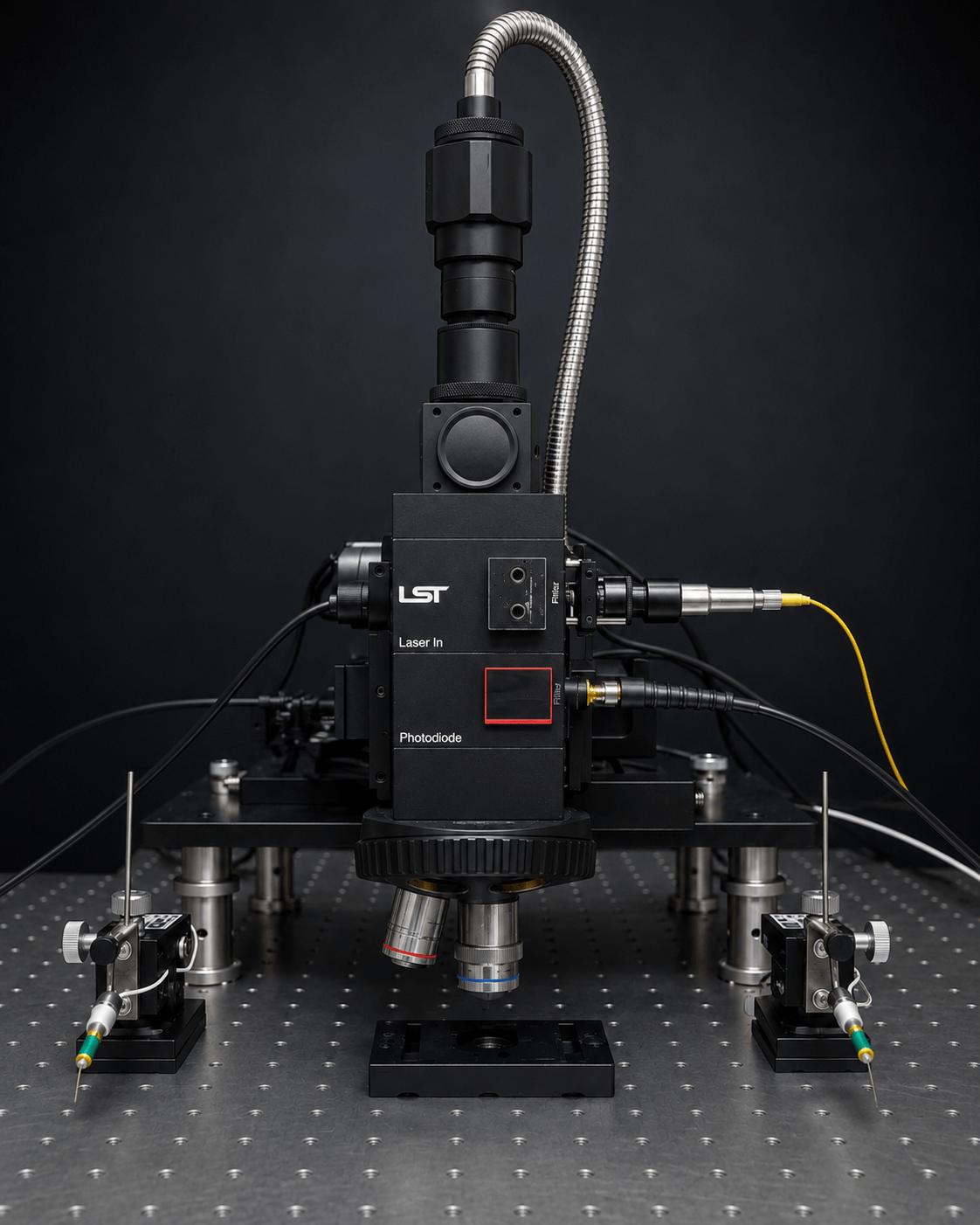
A modular optoelectronic workstation for spatially resolved mapping of photoresponse, charge transport and local electric-field distributions.
Request Information
01 / Overview
Material characterization
Spatially resolved insight into optoelectronic behavior.
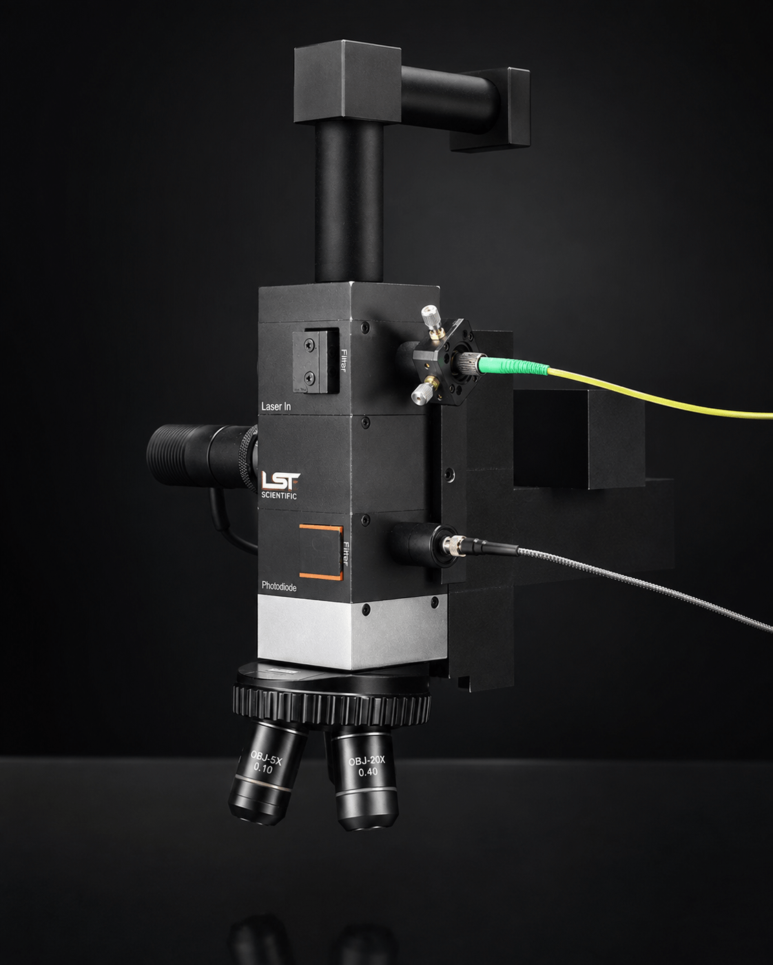
The LST SPCM combines an adaptable optical train, dual-axis galvanometer scanning and dedicated signal-recovery paths in a compact platform developed for advanced materials and micro-scale semiconductor devices.
- 01
Optical vector scanning for controlled spatial mapping
- 02
Photocurrent mapping for localized photoresponse measurements
- 03
Reflection mapping for spatial correlation and feature alignment
- 04
Integrated control and acquisition through purpose-built software

02 / Measurement
Photocurrent + reflection
Correlated maps from a single platform.
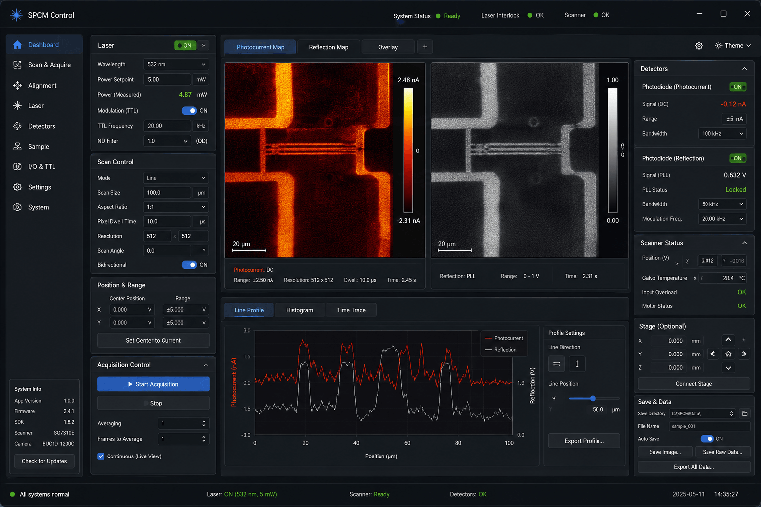
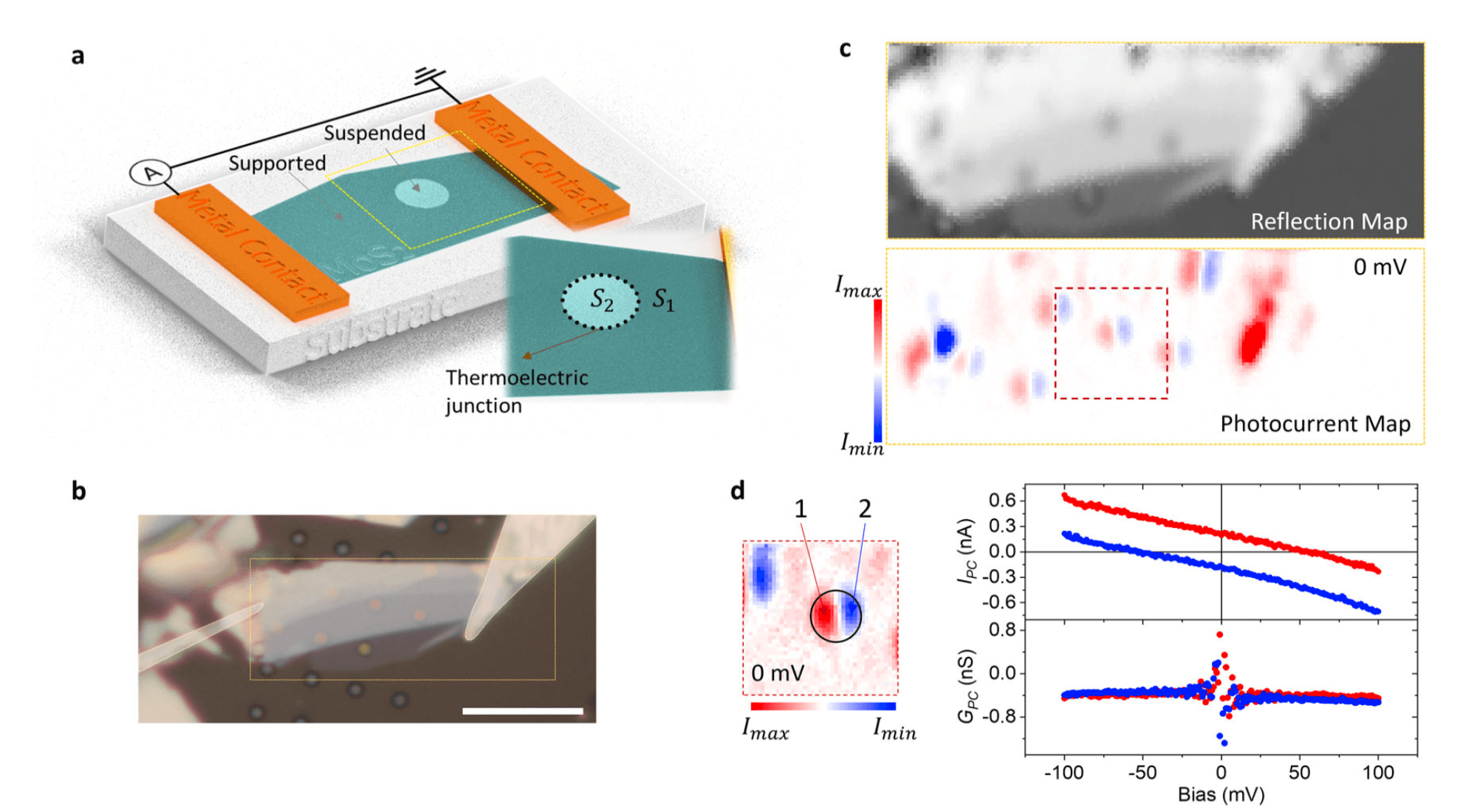
Concurrent photocurrent and reflection acquisition connects electrical photoresponse with optical structure, helping researchers align measured behavior with device features.
03 / Control software
Integrated acquisition
Control, visualize and inspect from one interface.
The cross-platform control suite brings scan setup, instrument synchronization, live mapping, line-profile analysis and data export into the measurement workflow.


04 / System architecture
Modular by design
Adaptable optics. Integrated control.
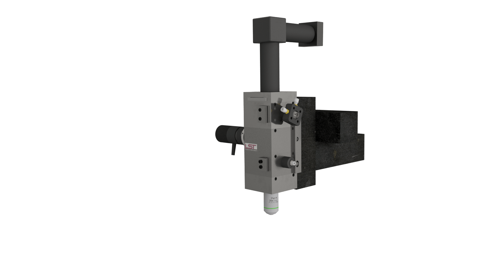
The open-frame architecture is designed around configurable optomechanics and infinity-corrected optics, allowing key optical and sample-handling elements to be adapted for specific research requirements.
- 01
Configurable excitation and optical components
- 02
Camera-assisted sample navigation and alignment
- 03
Dedicated signal recovery and instrument synchronization